China's 'trade-off' when producing non-EUV chips
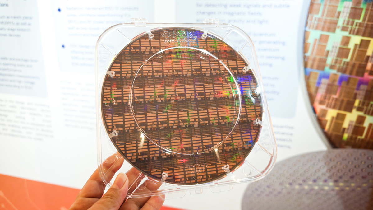
In recent years, EUV has been considered the biggest "bottleneck" in China's efforts to produce advanced chips, when this device could not be available in the country of billions of people due to US restrictions. Domestic semiconductor manufacturers mainly exploit DUV deep ultraviolet lithography technology, which is less modern.
"They seem to be at a similar stage to ASML in 2004," UBS analyst Francois-Xavier Bouvignies told Bloomberg.

Efforts to overcome difficulties
According to Tom's Hardware, before the ban was imposed, China had been preparing for the absence of US technology by actively purchasing semiconductor production equipment. Since 2012, domestic chip manufacturers have imported hundreds of DUV photolithography scanners from ASML, not including products purchased for multinational factories located in China.
At the end of September, a report from the Center for Technology & Statecraft (CTS) research organization in Washington showed that Chinese chip manufacturers had accumulated about 343 DUV chip production equipment in the period 2012-2026. 270 of them are ASML's Twinscan NXT:1980i, which has a resolution of 38 nm and the ability to overlap 2.5 nm matcher layers - an important index used to produce 7 nm chips.
In fact, even without the right to buy and use EUV machines, China has still made remarkable progress in recent times. Dismantling the Kirin 9000S chip model on the Huawei Mate 60 Pro in 2023, analysts realized it was manufactured by the Chinese company SMIC using the second generation 7 nm process without the need for an EUV machine. In August, TechInsight's analysis of the Kirin 9030 chip also showed that SMIC has pushed the DUV system closer to a density equivalent to 5 nm manufacturing technology.
In addition to imports, China also began producing immersion-type DUV photolithography machines developed by domestic enterprises. In July, The Information said that the production process involved many companies, including state-backed startup Shanghai Yuliangsheng Technology, with a production target of 5 machines this year and about 20 machines next year, expected to be handed over to SMIC, Hua Hong Semiconductor and CXMT.
Performance and cost barriers
According to experts, using DUV to produce advanced chips of 7 nm or less is not impossible. However, the key lies in the technique of creating multiple sample layers. Instead of printing the entire thing at once, which is very complicated, the Chinese manufacturer divides the design into many simpler patterns, then repeats the lithography process many times to create a circuit layer with a structure close to the original design.
Specifically, DUV has a wavelength of 193 nm, significantly longer than 13.5 nm of EUV. When manufacturing small structures, the factory must divide a circuit pattern into many small patterns, then perform many cycles of photolithography and etching to perfect the structure. This method helps DUV move towards advanced processes, but increases the number of stages, number of masks and the risk of errors. According to Reuters, switching from a 7 nm to 5 nm process using multiple patterning techniques can increase the number of production steps by about 20%.
“In the early stages of conversion, in terms of cost, three DUV exposures were equivalent to one EUV exposure,” photolithography expert Chris Mack, co-founder and CTO of Fractilia, explained to Tom's Hardware. "With three exposures, the costs of the two methods are almost equal. But when it is necessary to use four layers of 193 nm with DUV to replace one layer of EUV mask, EUV technology starts to have a cost advantage."
This method also affects chip quality and error rate. Each time a beam is "fired" onto the wafer, the new pattern must match exactly the circuit layer below. The more exposures, the greater the risk of bias. For example, if four 193 nm layers are used, coatings and process variations will accumulate through each step. According to CNA, each additional step creates an additional "opportunity" for errors in circuit size, uniformity or alignment. Small deviations can accumulate across multiple layers and reduce the odds of the chip performing as designed.
To reduce the risk, chip designers can increase the space between details on the chip, making the manufacturing process more stable. However, this method makes the chip larger, reducing the number of chips that can be produced per wafer - which costs tens of thousands of dollars per wafer.
"You don't sell wafers, you sell chips," Mack said. "The core issue lies in the number of chips that can be created on each wafer, how many chips achieve high performance, thereby determining production efficiency."
Some evidence shows that China's chip production efficiency is far behind that of foreign competitors. In June, investment bank Morgan Stanley estimated that Chinese DRAM maker CXMT could only make one-third as many chips per wafer as other firms using EUV machines.
"Access to the most advanced EUV lithography technology is a 'hard barrier' to China's memory development," commented Douglas Fuller, semiconductor researcher at Copenhagen Business School (Denmark). "In theory, manufacturers of advanced logic chips could find other improvements to reduce their reliance on EUV, but it is difficult to achieve high efficiency."
However, in the context of inaccessibility to EUV, DUV machines with China are still almost the only choice. According to Morgan Stanley, China's AI chip autonomy rate is expected to increase from 42% in 2025 to 70% in 2030. However, limitations in EUV and advanced software mean that China can only partially narrow the gap with the West.
"I have a hard time believing 3 nm or 2 nm technology would be economically viable without EUV," Mack added.