Intel shipped the first batch of chips from the $380 million machine
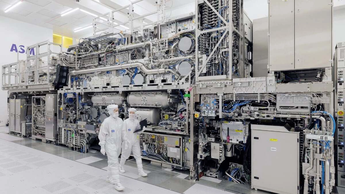
According to Intel Foundry - Intel's semiconductor processing business, "a small group" of Core Ultra Series 3 chips, codenamed Panther Lake, manufactured on the 18A process (equivalent to 2 nm) using ASML's High-NA photolithography machine, has just been shipped at the factory in Oregon (USA).
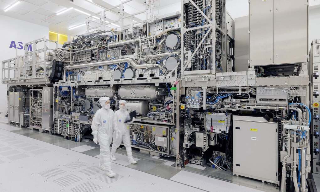
The ultra-ultraviolet photolithography system using large numerical aperture technology (High-NA EUV) is a technology developed by ASML and integrated in a machine called Twinscan EXE:5000. The whole thing weighs about 150 tons, equivalent to two Airbus A320 passenger planes and costs 380 million USD.
According to Interesting Engineering, there are currently only two products sold by the Dutch company to customers, one is shipped to Intel by the end of 2023, the other is said to go to TSMC. According to Monique Mols, ASML spokeswoman, the process of transporting and installing each machine requires 250 boxes and 250 engineers working continuously for 6 months.
Photolithography is the process of printing a circuit diagram onto the photosensitive surface of a silicon wafer by shining light onto the silicon wafer through a glass disc with a circuit diagram pre-drawn. The smaller the circuit, the more it requires shorter wavelength light rays, of which EUV ultraviolet rays are the most modern development today.
A higher aperture widens the EUV beam inside the machine before it contacts the silicon substrate. The wider the beam, the stronger the intensity, increasing the precision of the printed circuit and the density of components on the silicon substrate. According to ASML, High-NA EUV is the first photolithography machine in the world with the best digital aperture (NA) projection optical system today, able to print circuit lines only 8 nm thick, 1.7 times smaller and increasing component density by 2.9 times compared to the previous EUV line.
Intel's announcement marks the transition of High-NA EUV technology from the pilot phase to actual production. Intel and ASML also said the technology is being used on certain chip layers to collect data and optimize system setup and uptime before being deployed more widely on next-generation processes with high performance, high transistor density and improved manufacturing flexibility.
"The milestone reflects the close technical collaboration between Intel and ASML and shows how High-NA EUV technology can be integrated into advanced semiconductor manufacturing processes at scale," said Naga Chandrasekaran, Executive Vice President and General Manager of Intel Foundry.
Previously, ASML leaders also affirmed that High-NA EUV will play an essential role in AI. "AI technology requires huge data storage and processing capacity. This would not happen without ASML and the products we develop. AI is a big driver of our business," ASML CEO Peter Wennink told Reuters last year.
Intel is currently being positively received by Wall Street investors after a series of changes since CEO Lip-Bu Tan took power last year and launched bold strategies. Most recently, the company announced trial production of the advanced 18A-P chip. The "catalyst" for growth also comes from the US government when it invests and holds 10% of the company's shares in August 2025. Many American technology giants also poured money into Intel, such as Nvidia investing 5 billion USD, or Apple is said to have reached a preliminary agreement on chip production.