The solution helps China shorten chip production to a few seconds
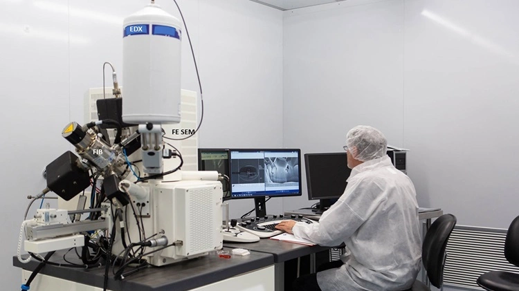
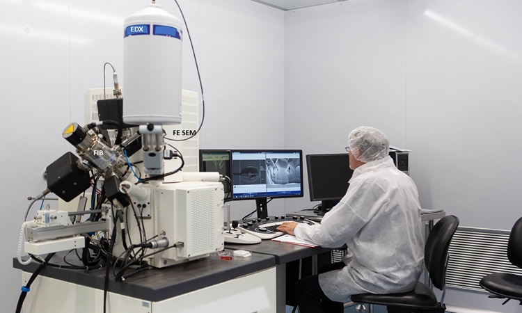
In research published on July 4 in the journal Advanced Materials, a research team from the Institute of Physics of the Chinese Academy of Sciences (CAS) in collaboration with the University of Hong Kong and several other Chinese institutions describes a manufacturing method that reduces the production time of complex 3D optical structures from hours to seconds. Instead of using a focused ion beam (FIB) to carve each structure one by one, graduate student Wang Yi and his colleagues developed a parallel manufacturing process that is capable of turning a two-dimensional (2D) model into a three-dimensional (3D) structure across an entire 10 cm wafer.
According to Interesting Engineering, FIB is commonly used for precise surface treatment and material analysis, but the research team's solution can overcome some of the disadvantages of this method. The method uses the FIB system to machine structures point by point with nanometer precision, but this serial process is very slow, expensive and not suitable for large-scale industrial production. The researchers sought to overcome the manufacturing challenge by replacing serial fabrication with a parallel process that transforms the entire wafer at once.
By expanding the optical structure into 3D, researchers can build more complex paths, achieve higher integration density, reduce crosstalk, and open up functions that are difficult to implement in 2D designs. According to the research team, the new production method achieves angular uniformity (the equal distribution of light intensity or color according to different viewing angles in space) of over 97% and the manufacturing time is 100 times shorter than FIB.
According to SCMP, instead of repeatedly machining each individual structure with FIB, the new technique exposes the entire wafer to a broad ion beam, causing thousands of pre-designed 2D nanostructures to fold into 3D geometries. Combining the use of a broad ion beam with origami-like self-folding, this method allows manufacturing across the entire wafer surface while maintaining nanoscale precision.
Optical chips are becoming central to the race to develop next-generation AI hardware. By transmitting data using light instead of electricity, optical technology can overcome bandwidth and power limitations. Many companies such as Intel, TSMC, Ayar Labs and Lightmatter are investing heavily in silicon photonics technology and optical interconnects, while several research organizations such as Belgium's Imec and Japan's NTT pursue photonic integration platforms. China is also expanding its investment in optical chips through CAS and companies like Huawei.